Accelerate Time to Signal and Power Integrity Compliance
Will Sparrow SI & PI Simulation Services Signal integrity is fundamental to any modern electronic system. The industry uses the term “integrity” as it means adhering to a code, remaining unimpaired, and being complete and undivided. If the waveform of the signal varies significantly from the original because of crosstalk, impedance mismatch, and losses, the receiver will not be able to read the signal, creating a signal integrity issue. That is why signal integrity engineering — analyzing and improving signal integrity issues — is an important part of designing integrated circuits (ICs), IC packages, and printed circuit boards (PCBs).
A system's signal integrity (SI) is a measure of how much an electrical signal changes between entering and exiting a circuit. For digital electronics, that signal is an electric current in which voltage varies between a high and a low value over time.
Delivering precise solutions for the most demanding high-speed designs
Advanced expertise in high-speed electronic design and signal integrity:
DDR3/4, SAS, PCIe3/4, Flash, Ethernet PHY, and Backplane interfaces
Optimization techniques for 28Gbps+ signal performance
Decoupling capacitor optimization for power integrity
Complex structures: PCB via, IC package & Connectors
Proficient in signal integrity analysis reports
Using high-speed scopes and TDR equipment
Our revolutionary methodology ensures optimal signal and power integrity through every stage of your design journey
Our comprehensive verification methodology ensures your design meets all performance requirements before manufacturing
Automated verification against manufacturability constraints
Advanced waveform analysis and margin assessment
PDN impedance and transient response verification
Pre-compliance assessment and optimization
Goal: Enhance DDR4 clock speed for better performance
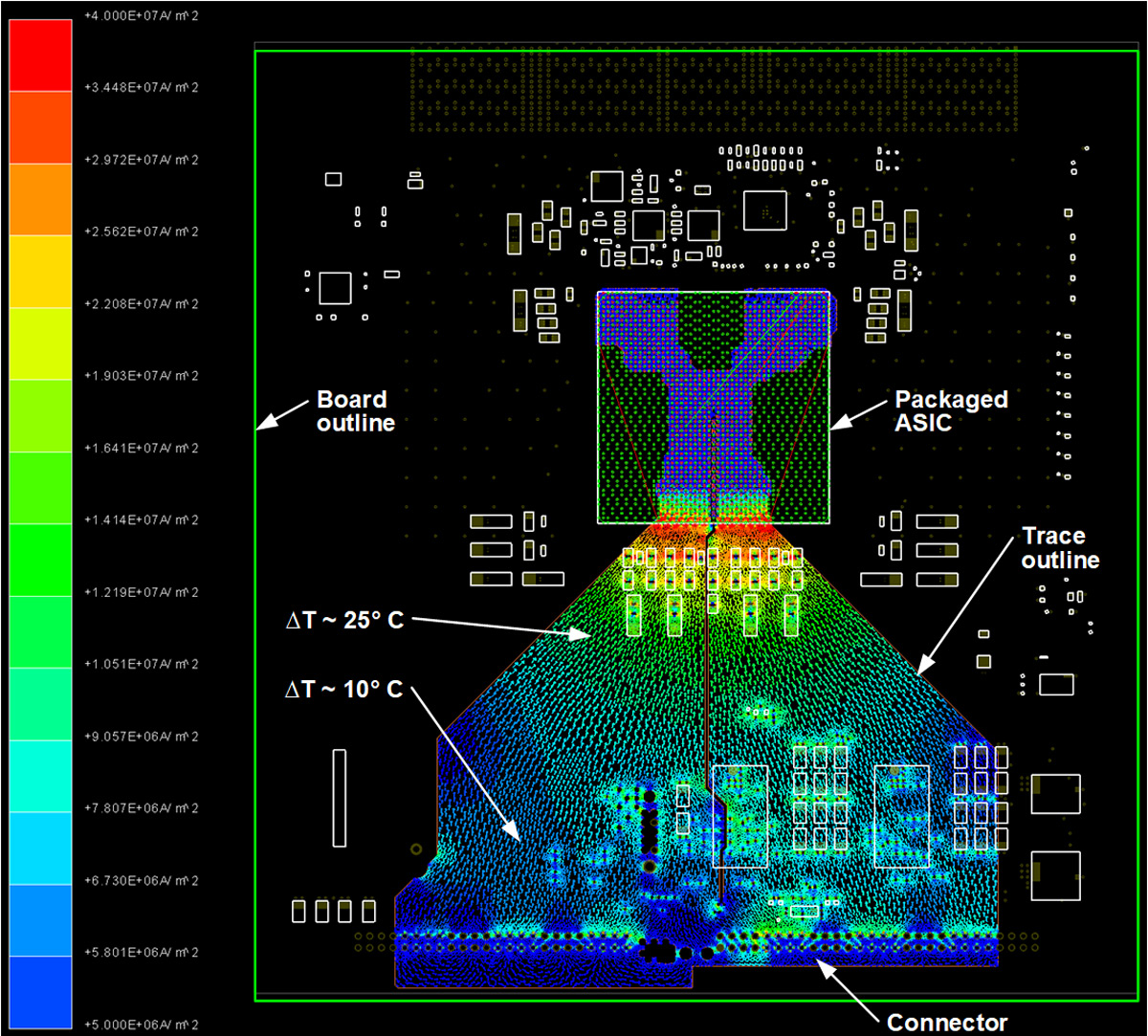
Increase in Current density(mA/mil2) at neckdown region, which cause power loss and heating on board
Increase the shape (Plane) width at the high current density region.
Goal: Evaluate voltage drop across a power delivery network (PDN) in a PCB
Reflection on DDR4_CLKN/P reduces the eye diagram margin, as CLK termination was present at FPGA side
Move the CLK termination scheme from Controller(FPGA) to Memory(DDR4) side
Goal: Ensure stable power to all chips in system with increasing PCB complexity and decreasing system size. Optimizing decaps locations and values in design phase will reduce risk of board re-spin. Stability of power rail to critical chips can be ensured by keeping the impedance of power rail below a specific target.
Goal: In high-speed designs, any small discontinuity in physical geometries along transmission path can degrade signal. This degradation includes loss of signal amplitude, change of signal rise time and increased jitter etc. PCB vias are a source of impedance discontinuities if not properly designed. The via stub, antipad size, drill hole size, and differential via pitch are important features for via impedance control.